

Manuscript accepted on : 22 December 2016
Published online on: --
Plagiarism Check: Yes
Ksenia Nikolaevna Denisova, Nastasiya Pavlovna Fantina, Alexander Sergeevich Ilin, Mikhail Nikolaevich Martyshov and Alexander Sergeevich Vorontsov
Physics Department, Lomonosov Moscow State University Leninskie Gory 1-2, Moscow, 119991, Russia.
DOI : http://dx.doi.org/10.13005/bbra/2406

ABSTRACT: The comparative analysis of the influence of femtosecond laser radiation on the structure and conductivity of undoped and boron-doped amorphous hydrogenated silicon was made in this paper. It has been found that the process of nanocrystals formation in an amorphous matrix by femtosecond laser radiation for undoped amorphous hydrogenated silicon samples begins at lower laser energy densities than for doped samples. Different conductivity of undoped and doped samples of amorphous hydrogenated silicon before femtosecond radiation becomes approximately equal upon radiation with laser fluence of 150-160 mJ/ cm2.
KEYWORDS: amorphous hydrogenated silicon; femtosecond laser crystallization; Raman spectroscopy
Download this article as:| Copy the following to cite this article: Denisova K. N, Fantina N. P, Ilin A. S, Martyshov M. N, Vorontsov A. S. Effect of Femtosecond Laser Radiation on the Structure and Conductivity of Boron Doped Amorphous Hydrogenated Silicon. Biosci Biotech Res Asia 2016;13(4). |
| Copy the following to cite this URL: Denisova K. N, Fantina N. P, Ilin A. S, Martyshov M. N, Vorontsov A. S. Effect of Femtosecond Laser Radiation on the Structure and Conductivity of Boron Doped Amorphous Hydrogenated Silicon. Biosci Biotech Res Asia 2016;13(4). Available from: https://www.biotech-asia.org/?p=17450 |
Introduction
Amorphous hydrogenated silicon (a-Si: H) has been successfully used for a long time for the production of solar cells, photodetectors, and widescreen displays. One of the main disadvantages of a-Si: H is the degradation of its parameters under illumination [1]. More stable electrical and photoelectric parameters can be achieved by the creation of nanocrystalline inclusions in a film of amorphous silicon [2-7]. This material (the material composed of amorphous silicon with crystalline silicon inclusions of nanometric size) was called nanocrystalline silicon (nc-Si:H). nc-Si: H can be obtain by femtosecond laser crystallization of a-Si:H [8-11]. This method allows crystallizing locally the selected areas of the a-Si: H film, minimizing hydrogen effusion from the film, as well as carrying out the so-called “cold” crystallization even on the fusible substrates.
Currently, femtosecond laser crystallization of a-Si:H is described in detail in the literature. In particular, there are the data on the effect of the femtosecond laser radiation on the structure, the hydrogen content, optical absorption, conductivity and photoconductivity of a-Si:H films [12-20]. However, the femtosecond laser crystallization was studied only for undoped a-Si: H. At the same time, elements of both p- and n-type are necessary for the creation of many semiconductor devices, so it is interesting to consider the effect of doping on the properties of a-Si: H, subjected to femtosecond laser crystallization.
The samples and methods of measurement
Two series of amorphous hydrogenated silicon films with thickness of 300 nm were prepared by plasma enhanced chemical vapor deposition from the gas phase of monosilane (SiH4) onto a quartz substrate coated with a layer of ITO. The temperature of the quartz substrate was 250 °C. During the preparing of second series samples diborane (B2H6) was also added to the reaction chamber, what resulted in the boron doped samples. Volume ratio of gases in the reaction chamber was [B2H6]/[SiH4] = 10-4.
The obtained films were exposed to femtosecond laser pulses with a femtosecond subterawatt complex on the basis of a Cr:forsterite laser. The wavelength of emission was equal to 540 nm, and laser pulse duration was 500 fs. The radiation was carried out with laser beam scanning the film surface. The scanning speed was v = 5 mm/s, the repetition frequency of pulses incident on the sample was ν = 200 kHz. The laser beam was focused onto the sample by means of an aspherical glass lens with a numerical aperture of 0.16. The focal plane was placed at a distance of 80 μm above the sample surface. The designations of the samples in the first and second series and values of the energy density of the used laser radiation are shown in Table 1.
Table 1: Designations of the samples in the first and second series and values of the energy density of the used laser radiation.
| No of Sample (first series) | Energy density of laser radiatoin, mJ/cm2 | № of Sample (second series) | Energy density of laser radiatoin, mJ/cm2 |
| 1-1 | 160 | 2-1 | 150 |
| 1-2 | 120 | 2-2 | 110 |
| 1-3 | 80 | 2-3 | 70 |
| 1-4 | 60 | 2-4 | 50 |
| 1-5 | 40 | 2-5 | 30 |
| 1-6 | 0 | 2-6 | 0 |
Measurements of Raman spectra were carried out with a spectrometer LabRam HR800 “Horiba Jobin Yvon”. Excitation of the samples was conducted by light with a wavelength of 632.8 nm. To measure the conductivity of the samples the aluminum contacts with area of 1 mm2 were deposited on their surface. The lower contact was an ITO film deposited on the substrate. To measure the conductivity of the films was used picoammeter Keithly 6487. The measurements were carried out at room temperature.
Results and discussion
Raman spectra of the films from the first and second series are shown in Figure 1, a and 1, b respectively. The volume fraction of the crystalline phase and the size of the nanocrystals were determined from the analysis of the Raman spectra in accordance to the procedure described in works [21-23].
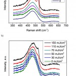 |
Figure 1: Raman spectra of the samples for the first series (a) and second series (b). Number of samples are shown in the figure |
Values of volume fraction of the crystalline phase and the nanocrystals size determined from the Raman spectra for samples from two series are shown in Table 2.
Table 2: Values of the fraction of the crystalline phase and nanocrystals size for samples.
| 1 series
a-Si:H |
2 series
a-Si:H(B) |
||||
| No of sample | Nanocrystals size, nm | Fraction of the crystalline phase, Xc, % | № of sample | Nanocrystals size, nm | Fraction of the crystalline phase, Xc, % |
| 1 | 6 | 22 | 1 | 4 | 7 |
| 2 | 6 | 14 | 2 | 4 | 5 |
| 3 | 6 | 3 | 3 | ── | 0 |
| 4 | ── | 0 | 4 | ── | 0 |
| 5 | ── | 0 | 5 | ── | 0 |
| 6 | ── | 0 | 6 | ── | 0 |
As can be seen in Table 2, in undoped a-Si:H films nanocrystals are formed at laser fluence of 80 mJ/cm2 and volume fraction of the crystalline phase may reach 22%. At the same time in boron doped a-Si:H films nanocrystals are formed at laser fluence of 110 mJ/cm2 and higher and volume fraction of the crystalline phase doesn’t exceed 10%. We can’t determine the cause of this difference clearly at now. However, it should be noted that according to [24-26] the samples of nc-Si: H with a volume fraction of the crystalline phase less than 10% and the nanocrystal size of 3-7 nm demonstrate the best parameters for solar energy application. The appropriate samples are obtained by laser crystallization of boron doped a-Si:H films. We can conclude that femtosecond laser crystallization of boron doped a-Si:H allows to obtain perspective material for solar energy application.
The dependences of conductivity on volume fraction of crystalline phase for both series are demonstrated in Figure 2.
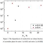 |
Figure 2: The dependences of conductivity on volume fraction of crysstaline phase for series 1 (a-Si:H) and series 2 (a-Si:H(B)) |
As can be seen before laser radiation the conductivity of boron doped films is larger than conductivity of undoped film by 2 orders. After laser treatment of samples the conductivity of all samples increases non-monotonically with increasing of laser fluence. The conductivity of boron doped films increases by 4 orders as conductivity of undoped films increases by 1-2 orders only. As the result after laser treatment with highest laser fluence the conductivity of undoped and boron doped samples become almost equal. It should be mentioned, for conductivity measurements the vertical configuration of electrical contacts was used and the distance between contacts was small (equal film thickness, 500 nm). The material of contacts can penetrate into the films and results to conductivity measurements error.
Conclusion
In summary, a-Si: H nanocrystals are formed in undoped films at laser fluence of 80 mJ / cm2 and the volume fraction of the crystalline phase reaches more than 20%. At the same time, crystallization of boron doped films starts at laser fluence of 110 mJ / cm2 and volume fraction does not exceed 10%. It can be assumed that the presence of boron influences the laser crystallization mechanism. So small volume fraction of the crystalline phase (less than 10%) at the femtosecond laser crystallization of boron doped amorphous silicon indicates the possibility of application in solar energy.
Before laser radiation the conductivity of boron doped a-Si: H films exceeds the conductivity of undoped a-Si: H films by 2 orders. After laser radiation the conductivity of a-Si:H(B) increases slightly with laser fluence. The conductivity of both doped and undoped films becomes alsmost equal at laser fluence of 150-160 mJ / cm2.
Acknowledgement
This work was supported by the Ministry of Education and Science of the Russian Federation (grant no. 14.604.21.0085, identification number RFMEFI60414X0085).
References
- D.L. Staebler, C.R. Wronski. Optically induced conductivity changes in discharge‐produced hydrogenated amorphous silicon.// Journal of Applied Physics, v. 51, p. 3262 (1980).
- C.R. Wronski, R.W. Collins. Phase engineering of a-Si:H solar cells for optimized performance.// Solar Energy, v. 77, p. 877 (2004).
- M.Y. Soro, M.E. Gueunier-Farret, J.P. Kleider. Structural and electronic properties of hydrogenated polymorphous silicon films deposited at high rate.// Journal of Applied Physics, v. 109, p. 023 713 (2011).
- J.P. Kleider, P. Roca i Cabarrocas. Reverse bias annealing of Schottky diodes: evidence for the lower defect density and better stability of polymorphous silicon compared to amorphous silicon.// J. Non-Cryst. Sol., v. 299–302, p. 599 (2002).
CrossRef - A.G. Kazanskii, P.A. Forsh, E.I. Terukov, J.P. Kleider. Photoconductivity of two-phase hydrogenated silicon films// Semiconductors, 2010, v. 44(4), 494-497 (2010).
- P.A. Forsh, A.G. Kazanskii, H. Mell, E.I. Terukov. Photoelectrical properties of microcrystalline silicon films.// Thin Solid Films, 2001, v. 383(1-2), p.251-253.
CrossRef - M.V. Chukichev, P.A. Forsh, W. Fuhs, A.G. Kazanskii. Creation of metastable defects in microcrystalline silicon films by keV electron irradiation.// Journal of Non-Crystalline Solids, v.338-340, p.378-381 (2004).
CrossRef - S.D. Sundaram, E. Masur. Inducing and probing non-thermal transitions in semiconductors using femtosecond laser pulses// Nature. Materials, v. 1, p. 217 (2002).
- J. Shieh, Z. Chen, B. Dai, Y. Wang, A. Zaitsev, C.-L. Pan. Near-infrared femtosecond laser-induced crystallization of amorphous silicon.// Appl. Phys. Lett., v. 85, p. 1232 (2004).
- X.C. Wang, H.Y. Zheng, C.W. Tan, F. Wang et al. Femtosecond laser induced surface nanostructuring and simultaneous crystallization of amorphous thin silicon film.// Opt. Express, v. 18, p. 19 379 (2010).
- B.K. Nayak, M.C. Gupta. Femtosecond-laser-induced-crystallization and simultaneous formation of light trapping microstructures in thin a-Si:H films.// Appl. Phys. A, v. 89, p. 663 (2007).
CrossRef - A.V. Emelyanov , A.G. Kazanskii, P.K. Kashkarov , P.A. Forsh, M.V. Khenkin, O.I. Konkov, E.I. Terukov, A.V. Kukin, M. Beresna, P. Kazansky Effect of the femtosecond laser treatment of hydrogenated amorphous silicon films on their structural, optical, and photoelectric properties // Semiconductors, v. 46, p. 749-754 (2012).
CrossRef - V. A. Volodin, A. S. Kachko, A. G. Cherkov, A. V. Latyshev, J. Koch, B. N. Chichkov. Femtosecond pulse crystallization of thin amorphous hydrogenated films on glass substrates using near ultraviolet laser radiation // JETP Letters, v. 93 (9-10), p. 603-606 (2011).
CrossRef - V. A. Volodin, A. S. Kachko. Crystallization of hydrogenated amorphous silicon films by exposure to femtosecond pulsed laser radiation // Semiconductors. v. 45(2), p.265-270 (2011).
CrossRef - A.V. Emelyanov, A.G. Kazanskii, M.V. Khenkin, P.A. Forsh et al. Visible luminescence from hydrogenated amorphous silicon modified by femtosecond laser radiation.// Applied Physics Letters, v. 101 (8), p. 081902 (2012).
CrossRef - M.V. Khenkin, D.V. Amasev, A.O. Dudnik, A.V. Emelyanov et al. Effect of laser wavelength on structure and photoelectric properties of a-Si:H films crystallized by femtosecond laser pulses. Journal of Nanoelectronics and Optoelectronics, v. 9, p. 728-733 (2014).
CrossRef - A. V. Emelyanov, A. G. Kazanskii, P. K. Kashkarov, O. I. Konkov, N. P. Kutuzov, V. L. Lyaskovskii, P. A. Forsh, M. V. Khenkin. Modification of the structure and hydrogen content of amorphous hydrogenated silicon films under conditions of femtosecond laser-induced crystallization// Technical Physics Letters, v. 40 (2) , p. 141-144 (2014).
CrossRef - A.V. Emelyanov, M.V. Khenkin, A.G. Kazanskii, P.A. Forsh et al. Femtosecond laser induced crystallization of hydrogenated amorphous silicon for photovoltaic applications. Thin Solid Films, 2014, v. 556, p. 410-413 (2014).
- M.V. Khenkin, A.V. Emelyanov, A.G. Kazanskii, P.A. Forsh et al. Effect of hydrogen concentration on structure and photoelectric properties of a-Si:H films modified by femtosecond laser pulses.// Canadian Journals of Physics, v. 92, p. 883-887 (2014).
CrossRef - A.V. Emelyanov, P.A. Perminov, P.A. Forsh, S.V. Zabotnov. Femtosecond laser crystallization of hydrogenated amorphous silicon films. // Nanomaterials and nanotechnology, v. 1, p. 40-46 (2012). [Russian]
- A.V. Emelyanov, A.G. Kazanskii, P.A. Forsh, D.M. Zhigunov et al. Photoluminescence features of hydrogenated silicon films with amorphous/nanocrystalline mixed phase. Journal of Nanoelectronics and Optoelectronics, v. 10, p. 649-652 (2015).
CrossRef - M.V. Khenkin, A.V. Emelyanov, A.G. Kazanskii, P.A. Forsh, P.K. Kashkarov, E.I. Terukov, D.L. Orekhov, P. Roca I Cabarrocas. Influence of the fabrication conditions of polymorphous silicon films on their structural, electrical and optical properties.// Semiconductors, v. 47, p. 1283-1287 (2013).
CrossRef - A.V. Emelyanov, E.A. Konstantinova, P.A. Forsh, A.G. Kazanskii, M.V. Khenkin, N.N. Petrova, P.K. Kashkarov, E.I. Terukov, D.A. Kirilenko, N.A. Bert, S.G. Konnikov. Features of the structure and defect states in hydrogenated polymorphous silicon films. JETP Letters, v.97 (8), p. 536 – 540 (2013).
CrossRef - M.V. Khenkin, A.V. Emelyanov, A.G. Kazanskii, P.K. Kashkarov, P.A. Forsh. Photoelectrical and optic properties of polymorph silicon films, obtained at different temperatures.// RSREU Bulletin. v. 42 (4), p. 47 – 51 (2012). [Russian]
- A.G. Kazanskii, P.A. Forsh, M.V. Khenkin, E.I. Terukov. Specific features of photoelectric and optical properties of amorphous hydrogenated silicon films produced by plasmochemical deposition from monosilane-hydrogen mixture.// Semiconductors, v. 45(4), p. 510-514 (2011).
CrossRef - P. Roca i Cabarrocas, A. Fontcuberta i Morral, Y. Poissant. Femtosecond laser induced surface nanostructuring and simultaneous crystallization of amorphous thin silicon film.// Thin Sol. Films, v. 403-404, p. 39 (2002).
CrossRef

This work is licensed under a Creative Commons Attribution 4.0 International License.


