

Manuscript accepted on : 28 June 2018
Published online on: 29-06-2018
Marjan Abbasi
M. A. student of physics, solid state, payamenoor Tahran East, Iran Tehran.
Corresponding Author E-mail: marjanabasi796@gmail.com
DOI : http://dx.doi.org/10.13005/bbra/2635

ABSTRACT: Creating light source has always been an interesting matter in the field of optical devices. One of the activities in this field is the effort to build optical diodes and High-efficiency lasers. The aim of this study was to use GaN-based diode lasers with Shaped patterned hemisphere algorithm using Poynting vector analysis can cause modification in output light efficiency. In this article we get to know with time-based finite difference method as one of the analyzing and electromagnetic equations solving and also check out parsing method and data analysis by using APSYS simulator. Results of simulation not only infer that PSS can decrease reflexive angle in the form of hemisphere, but also increase the Transmission angle and all this so that light reflection on it to be increased, moreover, increasing cone in its formula causes increase in light performance.
KEYWORDS: Diode Simulation; GaN-Based Diode Lasers; Patterned Hemisphere; Pointing; Sapphire Layer
Download this article as:| Copy the following to cite this article: Abbasi M. Simulation of a Gan-Based Optical Diode with Sapphire Sub-Layer Which is Shaped Patterned Hemisphere, using Poynting Vector Analysis. Biosci Biotech Res Asia 2018;15(2). |
| Copy the following to cite this URL: Abbasi M. Simulation of a Gan-Based Optical Diode with Sapphire Sub-Layer Which is Shaped Patterned Hemisphere, using Poynting Vector Analysis. Biosci Biotech Res Asia 2018;15(2). Available from: https://www.biotech-asia.org/?p=30099 |
Introduction
Optically, light crystal’s structure is composed of dielectrics which are meant to be in one, two or three dimension that refractive index changes periodically in them, This periodicity causes prohibited areas or band gap for electromagnetic waves. By choosing proportion crystal parameters, this band gap is adjustable for various wavelengths. Prohibited areas cause these crystals to be used for different purposes like building mirrors, momentum waves, filters, etc.
Photonic crystals depending on Frequency coefficient to be in 1,2 or 3 dimension are categorized into three types of photonic crystals:1,2 and 3 respectively. By creating Photonic crystals energy bar, they have the ability of limiting the radiation of photon modes. Creating adjustable energy gap in them gives us the capability of being involved in the selection and determination the amount of receiving power. Furthermore, Photonic crystal by the ability of Photons Auto glowing controlling within its energy gap is able to prevent light emission in all directions. In case of naming some of updating Photonic crystals uses can mention something as follows: high-quality, coefficient, optical oscillators, filters, Prisms, polarizers, optical smithereens. One of the important use in photonic crystals is optical diode structure, where solid mode has high external efficiency. At the moment, optical solid-mode diodes in internal optical connection inside the computers, printers, display screens, have different usages. nevertheless, although Internal quantum efficiency is almost 100%,but most energy resources are customized to the semiconductor conductive modes and just a few of it is sent out to the outside perimeter, and because of this reason there are a lot differences between semiconductor refractive index and outside perimeter. Different ways have been proposed to solve this problem so far, for instance, using certain material layers by integration to modify light path or using photonic crystals by limited thickness (like inserting Photonic crystals in LED)in checking Quantum wells: GaN and In GaN many researches have been done. Literally, by changing carriers between potential wells and being limited which are as a result of thin layers of semiconductors, Quantum star effect or Quantum well occurs. Quantum well is one of the Quantum semi-conductor systems which charge carriers movement are limited in one side and free on the other 2 sides. One dimension Quantum limit in these structures causes vastness in energy levels and produces electronic and optical new Features. According to recent studies, for discussion about electrical Field in Quantum well and load accumulation in Quantum well’s margent (GaNand In GaN) by well depth enhancement, the potential drop is linearly increased and the field remains constant. Whereas after that potential decreases and also field does, moreover, in multiplex Quantum well. Putting wells together causes creating a significant field in the dam layers. Anyway, a lot of techniques have been developed to improve LED function depending on GaN like upgrading level (Qi, et al., 2009), Photonic crystals techniques (Fu, et al., 2011), coherent lateral growth(mark and,1998) and Sapphire layer techniques(LI,2006). At the moment PSS techniques (Sapphire layer hemisphere) is largely paid attention, hence it can cause increase LEDs external quantum efficient (EQE) because of light efficiency enhancement extraction (LEE) and internal quantum efficient (IQE). Recently, utilizing Sapphire layer pattern (PSS) in optical diodes based on GaN implies that it will be replaced by inflamed bulbs and fluorescent lamps (Muramoto, et al., 2011) and it’s generally considered. Because not only it reduces density in GaN layer but also output light efficiency correction which causes increase in external LED power based on the GaN (LI 2010). In addition, some processes in which are used in the structure of semiconductor instruments can be written as follows: oxidation, adding impurity (which is done in either infiltration or ion implantation) film deposition, gas phase epitaxy (which is a lot important in LED structure) vacuum deposition, which is Photolithography and thermal annealing. In LED structure light is emitted when Electrons and Protons are flown as majority carrier. They are injected to the other side of the junction and re-combined at the junction near that.it makes the re-combination radiant event. LED element has various structures whereas the most common a small LED structure contains formatting plus semi-conductor chip. Since the light is released from the sideways and a reflector bowl is used in front of the chip to propagate the light straight among a molded polymeric lens to access to GaN matter by high-functioning was the main discussion of many analysis. Optimizing white emitted LEDs is a topic which ongoing attempt is in progress about it. There are a lot of phosphorous materials that have particular emission spectrum. It can be used in 2 LED chips or more to use it for produce white spectrum. Since the In GaN Blue LEDs are extremely efficient,the eagerness of white LEDs has led to the development of LEDs what turns blue light into white light. There are several studies about in LEDS and lasers based on InGaN. Checking group Studies out in universities and Industry provided possibility of making LED of In GaN. Blue LEDs are made of a GaNP GaN / n In GaN / n dual structure. High In GaN highlights The blue, green, yellow In GaN LEDs brightness by quantum well are being grown based on nitrides on sapphire substrates. White LEDs can be stimulated by external shining materials used in energetic blue LEDs. The stimulated phosphorus (shining matter) by volumetric light emits yellow light. White light is a mixture of blue light from In GaN and yellow light from white phosphorus. Here are some of the specifications mentioned in LED structure based on In GaN/In: voltage-current curve, two BIAS factors which influence on diode- efficiency impurity. About impurity, the process follows a Gaussian curve and doing impurity operation does not have always a positive effect. Hence, optimization is absolutely essential to obtain the best measure as much as impurity length the photon emission has been increased as much as wavelength has been transferred to be invisible.so for a limited wavelength must not overrun a specific length increasing this impurity can increase efficiency however increasing the net can increase efficiency. A case reported the impact of the shape (Hsu, 2012), phase space (Song, et al., 2007) and the size (Xia, 2015) and showed that Pss is sensitive to the LED function based on GaN. Therefore accurate simulations on a GaN-based LED along with the PSS are essential for future development of this structure. Although some theoretical studies have been carried out using beam tracing techniques, Based on geometric optics (Lin,2012) However when the size of the PSS pattern is compatible with the wavelength of the diffusion of the LED structure, Light wave properties such as the effects of wave interference and light parsing are not considered. Thus, in this research to achieve a solution to increase light efficiency to simulate GaN-based LEDs along with PSS.
Methodology
In this research a GaN-based LED with a PSS hemisphere is numerically investigated in two dimensions by the updated APSYS simulation program. A light Poynting vector is used to generate reflection angles and transmission depending on the position near the common PSS level for tracking radiation to improve the accuracy of GaN-based LED simulations. APSYS simulator tool, The finite element-based simulator is a self-coherent Poisson Schrödinger equation. Current constancy equations, heat transfer equations and hydrodynamic equations include K. P models for MQW band structure, quantum tunneling model for heterogeneity, heat flow model for self-heating, model of radiation detection based on Fresnel equations for photon extraction, The FDTD model for calculating the emission of electromagnetic waves in space, spontaneous models and piezoelectric polarization for the internal electric field also solves the combination of SRH and recombination if the carriers are dissolved.
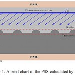 |
Figure 1: A brief chart of the PSS calculated by FDTD
|
Two PMLs with a 3 micrometers thickness on top and bottom PSS are used to absorb electromagnetic waves in the vertical direction. with a flat current source for the FDTD above the is treated PSS as a waveguide with a variable angle of zero to 180 degrees and a wavelength of 0.4 micrometer. Two close virtual transitions and reflections to the PSS Poynting, transmission and reflection of light are also defined at different angles of incidence in the PSS interface. Poynting vector directions are used as transducer transitions and light reflection in different positions of impact in PSS because the Poynting vector shows the direction and energy flux of the electromagnetic field energy which can include the effect of the light-wave characteristics of the PSS interface. In the tracking radiation simulation. The self-propagating power of the LED on the page source in the active area with 10 averaging spatial points that initially can emit 10000 light rays each. we assume that the hemisphere pattern is arranged at a distance S along the x direction of its original point as shown in figure 2.
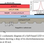 |
Figure 2: a schematic diagram of a GaN-based LED with PSS hemispheres showing a drop of its electroluminescence spectrum at 40 mA
|
Geometrically interacts with the emission of light emitted in all LED devices based on Fresnel equations but when the light ray strikes the PSS interface, Its geometric optics parameters derive from FDTD results based on the angle of incidence and its impact position in the PSS interface. The AlGaN and InGaN indexes are calculated according to the Vegan rules. The N and P electrodes are considered transparent. The energy gap of InxGa1-xN band is estimated by equation (1)
Eg (x) = x Eg (InN) + (1-x) Eg (GaN) – bx(1-x) (1)
In equation where (1), Eg (GaN) = 3.44eV is GaN gap-band energy and Eg (InN) =0.71eV is InN gap-band energy.b is the bending parametr of Inx Ga1-x N which is adjusted on 3.0 eV. The band offset rate for InGaN / GaN is assumed to be 3.7.
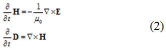
A numerical method for electromagnetism based on the solution of equations is the finite difference time domain (FDTD). The primary advantage of the FDTD is being straightforward to work with rectangular grids and the field components can be calculated directly and without needing to invert the matrix. The field equations are obtained naturally stable at certain times. the FDTD algorithm is effectively used for microwave issues such as waveguides, split lines and microstrip circuits. One of the greatest scientific achievements of the nineteenth century is Maxwell’s equations. Earlier, because of the lack of strong computing capabilities like today’s computers, most of attempts in resolving equations were spent for Single-Frequency Form or Time Harmonic. Until a simple version with very interesting numerical features but with a large computational burden was presented for solving the Maxwell equations in the time domain. This method has been developed and could enter many fields of science and technology so far. The Kerl Maxwell equations have no assumption that the electrical and magnetic conductivity σ and * σ are not present and the medium does not have magnetic property which means µ(r)=µ0 can be written as:
If we customize (I,j,k)indexes to the cell coordinates in FDTD method in figure 3, (iΔx, jΔγ, kΔz) will be coordinate of the top left and bottom of the cell:
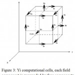 |
Figure 3: Yi computational cells, each field component is surrounded by four components
|
According to the Yi marketing, the components of the discrete field can be written as follows:
![]()
Thus, each function depending on location and time can be written as follows:
![]()
By applying the central finite difference and definitions above, the discrete form of the Maxwell equations (2) would be as follows:
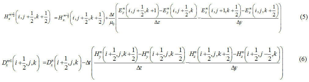
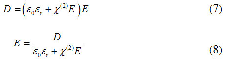
There are also some alternative field components with similar relationships which Δz = Δγ = Δx = Δ applies depending on the size of cell in three columns x,y amd z respectively. Δt is the time of calculation as well. for nonlinear optical materials that have nonlinear second-order response,a profitable aquation like this expresses the relation between the displacement field D and the electric field E as it follows:
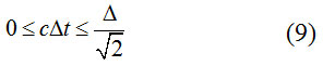
of course in order to disconnect this equation, the electric field on the right should use a value in the past time to calculate the field at the present time. Using input waves with TE or TM polarization in two-dimensional photonic crystal investigations is the most common method to reduce the equation sentences(3) and (4) and finally reduce the volume and time of the calculations.in case of using algorithm Yi in FDTD method you it has to be considered that this conditional stability algorithm is expressed in terms of two-dimensional problems. It can be written as:
The last and the most important point in this method is simulation of waves in a computational cell space to an infinite space for getting close to a numerical solution for the matter of physical reality. Which in this case is used as an aggregate boundary (ABC) called UPML and now, it is the best absorbing condition. the cross-equation solves the Poisson equation and equations of electrons current and hole. Poisson equation can be written as follows:
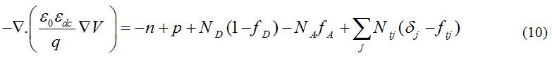
In equation(10), V is electric potential, εo is dielectric vacuum coefficient, εdc is fixed low frequency DC or dielectric q is electronic charge, n is electronic concentration, p is hole concentration, ND is Shallow donor density, NA is shallow acceptor density, fD is occupy level of the helper,fA is Occupy the receptive level,Ntj is deep trap density of j, ftj is deep layer dust of j, jδ 1 is a trap for donor and 0 is a trap for acceptor. The current persistent equations for electrons and holes are can be written as follows:
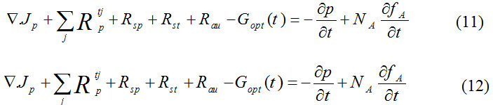
In the above equations, Jn and Jp represent the electron density and the hole of the current flow, respectively. The notes Rntj and Rptj are the rate of electron nucleus and hole in the unit volume through the deep trap j, Gopt, the light production rate and Rst, Rsp and Rau are respectively the spontaneous recombination rate, the stimulated recombination rate, and the Auger recombination rate per unit volume. These equations control the electrical behavior of a semiconductor device.
Theoretical Analysis
For a gallium-nitride-based LED, the recombination rate is calculated as follows:
R = An + Bn2 + Cn3 + f (n) (13)
In which n represents the concentration of carrier n and f (n) is the carrier leakage and A represents Shakley-Reed-Hull, B is the radiation coefficient and C is the screw coefficient. At low and medium flow rates, the carrier leakage is negligible, so the output power of light (P) PαBn2 and current (I) is expressed as follows:
I α An + Bn2 + Cn3.
By definition
![]()
The quantum efficiency can be expressed as follows:
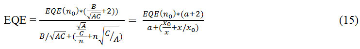
In this equation, x0, n0, EQE (n0) are the values in the maximum of external quantum efficiency.
The parameter
![]()
can be obtained by matching the external quantum efficiency against the root of the square the light output curve around the maximum external quantum efficiency at the low and intermediate flow level. Also, the maximum internal quantum efficiency is:
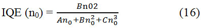
Therefore, the related light extraction efficiency can be concluded:
LEE = EQE (n0) / IQE (n0)
Light extraction efficiency (LEE) usually is considered to be constant based on various flow injection. Using the external quantum efficiency obtained from the optical power versus the curve of flow injection, it is possible to obtain internal quantum efficiency by dividing external quantum efficiency by light extraction efficiency. Figure 1 presents the process of analysis of typical connections.
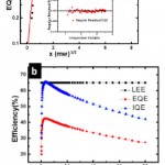 |
Figure 4: Quantum efficiency as a function of the flow injection
|
Poynting Vector
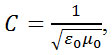
Electromagnetic radiation exists in any of the space regions. Therefore, it is obvious that the radiant energy is considered in a unit of volume or energy density (u). Suppose that the electric field can save energy somehow. This is a logical assumption because this property is somewhat close to the physical reality that if the field has the energy, it has something within itself. In addition, because the classical field is continuous, its energy is also lasting. Now we have to see where this energy is directed. When a parallel capacitor (capacitor C) is charged with the voltage V, it can be assumed that the stored energy
![]()
in it due to reciprocating charge has covered gap statically in the E field. With a surface A and a distance d, (C = ε0 A / d), the energy per unit volume in the gap is
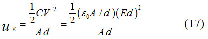
So, it can be concluded that the energy density of the space field E is equal to
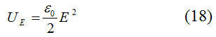
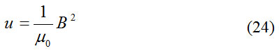
Similarly, the density of the field B can only carry the current i by considering a hollow or induction coil (induction from the current i). The magnetic induction capacity of a solenoid with the cross-sectional of the surface A and the length l with n rotations per unit length is equal to L = µ0n2lA. The magnetic field inside the coil is B = μ0nI, and therefore the energy density in that region is
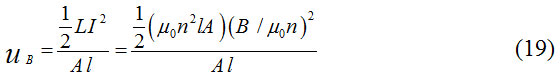
And with the same logic, it is proved that the energy density of any field B in the empty space is equal to
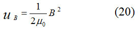
The equation E=CB is specifically used for the plane waves, but it can be applied to different waves. By use of this equation and this fact that
it can be proved that
uE = uB (21)
The energy flow is evenly divided between the electric field and magnetic field via space. Since
u = uB + uE (22)
u = εo + E2 (23)
This equation is equal to
It should be noticed that the fields change and u is a function of time. To show the electromagnetic energy flow associated with a motion wave, S represents the energy transfer per unit time (power) in a single region and its unit in the SI system is (W / m2). Assume an electromagnetic wave with velocity c through a region A crosses during a very short time interval Δt. So, the only energy in the cylinder volume u (cΔtA) passes through A. Thus
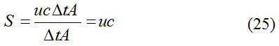
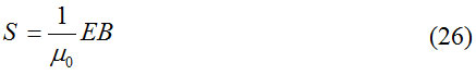
According to the equation (23), it can be said that
Result and Discussion
Electrically, a diode passes the current through itself when it is ready to work by setting the voltage (biasing) in the correct direction (+ to the anode and – to the cathode which is called the forward bias). The voltage that causes the diode to start conducting the electric current is called the threshold voltage, which is about 0.6 to 0.7 volts (for silicon diodes) and 0.02 to 0.3 volts (for a germanium diode). But when the reverse voltage is connected to the diode, (+ to the cathode and – to the anode, which is called the inverted bias), it does not flow any current, except for a very small current known as a “leakage current” and is about a few microamperes or even is less. This flow rate can be ignored in most electronic circuits, and it does not affect the behavior of other circuit elements. As the crystal material used in making the diode is more structurally regular, the diode is better and the leakage current will be less. The amount of leakage current in diodes with a new technology practically tends to zero. But the important thing is that all the diodes have a threshold for the maximum reverse voltage, that if the reverse voltage exceeds that, the diode burns (the crystal melts) and pass the flow in the opposite direction. This threshold voltage is referred as “breakdown voltage”. If the reverse voltage of the diode increases to a certain degree, the reverse current in the diode starts to increase rapidly. The phenomenon that occurs in this case is called “failure phenomenon” and the voltage, which at this phenomenon begins, is referred to the breakdown voltage and is showed by VBR. The voltage of the diode depends on the structure of the P-N junction and its impurity concentration in a relatively well-known manner; Breakdown diode can be due to one of the two phenomena, Avalanche breakdown and Zener breakdown. The likelihood of a breakdown phenomenon is higher in silicon diodes with a breakdown voltage higher than 6 volts. While Zener breakdown as a dominant phenomenon is found only in diodes with a voltage breakdown lower than 6 volts.
Due to the non-linearity characteristic of the diode, two types of resistance can be defined for the diode. These resistances are the static resistance (Rs) calculated in DC current and dynamic resistance calculated in AC current. Ohm resistance in a diode is calculated by dividing the voltage of the two terminals of the diode to the current flow. The resistance of the diode varies to direct current and alternating current. The resistance of the diodes against to the direct current is called the static resistance.
Recently, GaN diodes have been widely evaluated because of the tremendous potential to use for light energy applications to replace the incandescent light bulb and fluorescent lamp and significant progress has been made. However, the rapid reduction of internal quantum efficiency (IQE) with the increase in the current knowing as “performance reduction” is the dramatic barrier to improve the performance of LED. Several physical mechanisms have been proposed, including Auger recombination, carrier duct, polarization effects, heating connection, and injection of a weak signal through a hole and electron leakage as potential causes of performance reduction.
This LED is included a semiconductor material chip connected to the impurities to create a p-n junction. As in other diodes, the current flows easily from the p side, or anode, toward n, or cathode, but not in the opposite direction. Chargers – electrons and holes – are connected to electrodes of different voltages. When the electrons collide with the hole, it falls to a lower energy level and releases energy in the form of a photon. The wavelength of the light and its color depend on the energy of the band gap of the bonding material. In silicon or germanium diodes, electrons and holes are usually reconstructed with non-radiation transduction that does not produce any light emission because these are indirect materials. The materials used for the LEDs have a direct gang gap with energies which are close to the light close to the infrared, visible, or ultraviolet light. The development of LEDs began with infrared devices made with gallium arsenide. Advances in material science make devices with fewer wavelengths that emit light in various colors. LEDs are usually made on a n-type structure and an electrode which is attached to the p-type plate and is located on its surface. P-type regions also occur, whereas they are less common. Also, Many commercial LEDs, especially GaN / InGaN, use sapphire infrastructure.
Conclusion
According to ever-increasing speed of science advances, especially in the field of electronics, the need for the speed of data transfer and processing and its storage is increasingly seen. The GaN semiconductor is widely used in high-frequency electronic components. This widespread use is due to the large gap energy of this type of semiconductors. The GaN-based light-emitting diodes (LEDs) with hemisphere patterned sapphire substrate (PSS) are numerically investigated using radiation detection method and FDTD method. Reflection and position-dependent transfer angle in the interface sapphire substrate is extracted from the calculation of FDTD based on the Poynting vector. The simulated results show that PSS the hemispherical PSS can reduce the reflection angle, increase the transmission angle and increase the reflectance of the light incident on it, and also enlarging the escape cone at its interface causes the increase in the brightness of the light extraction efficiency. In addition, the size of the hemisphere pattern has a significant effect on the exposure efficiency of the light of GaN-based LED with a hemisphere PSS. It has been determined that the optimum radius for the hemisphere pattern is related to the wavelength of the device, due to the strong effect of the properties of the light wave in the PSS interface.
The GaN-based light-emitting diodes (LEDs) with hemisphere patterned sapphire substrate (PSS) by using pointing vector analysis can improve light-output efficiency. In this paper, the finite-difference time domain (FDTD) as one of the tools for analyzing and solving electromagnetic equations is explained and also the data analysis is explained using the APSYS simulator. The simulated results of this study indicate that the hemispherical PSS can reduce the reflection angle, increase the transmission angle and increase the reflectance of the light incident on it, and also enlarging the escape cone at its interface causes the increase in the brightness of the light extraction efficiency.
References
- Fu X. X, Kang X. N, Zhang B, Xiong C, Jiang X. Z, Xu D. S & Zhang G. Y. Light transmission from the large-area highly ordered epoxy conical pillar arrays and application to GaN-based light emitting diodes. Journal of Materials Chemistry. 2011;21(26);9576-9581.
CrossRef - Fujii T, Gao Y, Sharma R, Hu E. L, DenBaars S. P & Nakamura S. Increase in the extraction efficiency of GaN-based light-emitting diodes via surface roughening. Applied physics letters. 2004;84(6):855-857.
CrossRef - Hecht E. Optics, Fifth edition, Global Edition, Adelphi University. 2017.
- Marchand H, Wu X. H, Ibbetson J. P, Fini P. T, Kozodoy P, Keller S & Mishra U. K. The microstructure of GaN laterally overgrown by metalorganic chemical vapor deposition. Applied Physics Letters. 1998;73(6):747-749.
CrossRef - Muramoto Y, Kimura M, Dempo A, Nouda S, Fukawa Y & Sakai S. High‐efficiency UV LEDs and RGB white LEDs for lighting and LCD backlights. Journal of the Society for Information Display. 2011;19(12):907-912.
CrossRef - Pimputkar S, Speck J. S, DenBaars S. P & Nakamura S. Prospects for LED lighting. Nature photonics. 2009;3(4):180-182.
CrossRef - Qi S. L, Chen Z. Z, Fang H, Sun Y. J, Sang L. W, Yang X. L & Yu T. J. Study on the formation of dodecagonal pyramid on nitrogen polar GaN surface etched by hot H 3 PO 4. Applied Physics Letters. 2009;95(7):071-114.
- Song J. C, Lee S. H, Lee I. H, Seol K. W, Kannappan S & Lee C. R. Characteristics comparison between GaN epilayers grown on patterned and unpatterned sapphire substrate (0001). Journal of Crystal Growth. 2007;308(2):321-324.
CrossRef - Tadatomo K, Okagawa H, Ohuchi Y, Tsunekawa T, Imada Y, Kato M, & Taguchi T. High output power InGaN ultraviolet light-emitting diodes fabricated on patterned substrates using metalorganic vapor phase epitaxy. Japanese Journal of Applied Physics. 2001;40(6):L5-83.
- Xia C. S, Sheng Y, Li Z. S & Cheng L. Simulation of GaN-Based Light-Emitting Diodes With Hemisphere Patterned Sapphire Substrate Based on Poynting Vector Analysis. IEEE Journal of Quantum Electronics. 2015;51(5):1-5.
CrossRef - Kawakami Y, Narukawa Y, Omae K, Fujita S & Nakamura S. Dimensionality of Excitons in InGaN‐Based Light Emitting Devices. physica status solidi (a) . 2000;178(1):331-336.
CrossRef - Nishida T, Saito H & Kobayashi N. Efficient and high-power AlGaN-based ultraviolet light-emitting diode grown on bulk GaN. Applied Physics Letters. 2001;79(6):711-712.
CrossRef - Billeb A, Grieshaber W, Stocker D, Schubert E. & Karlicek F, Jr R. F. Microcavity effects in GaN epitaxial films and in Ag/GaN/sapphire structures. Applied physics letters. 1997;70(21):2790-2792.
CrossRef - Bergh A , Hill M , Saul R. H and Plains S, Patent U.S. No. 1973;3:739-217.
- Minsky M. S, White M & Hu E. L. Room‐temperature photoenhanced wet etching of GaN. Applied Physics Letters. 1996;68(11):1531-1533.
CrossRef - Cao X. A, Pearton S. J, Zhang A. P, Dang G. T, Ren F, Shul R. J & Van Hove J. M. Electrical effects of plasma damage in p-GaN. Applied physics letters. 1999;75(17):2569-2571.
CrossRef - Ohba Y & Hatano A. A study on strong memory effects for Mg doping in GaN metalorganic chemical vapor deposition. Journal of Crystal growth. 1994;145(1-4):214-218.
CrossRef - Wierer J. J, Steigerwald D. A, Krames M. R, O’shea J. J, Ludowise M. J, Christenson G & Götz W. High-power AlGaInN flip-chip light-emitting diodes. Applied Physics Letters. 2001;78(22):3379-3381.
CrossRef

This work is licensed under a Creative Commons Attribution 4.0 International License.


